| There is a lot of buzz in the computer industry about so-called three-dimensional (3D) chips, promising higher performance with lower energy consumption, and paving the way for exascale computers (which would represent a thousandfold increase in performance over the current petascale architecture). However, these chips are not intrinsically built, true 3D chips; rather, they are stacked layers of up to 100 separate chips (see: "New types of adhesives for 3D semiconductors could lead to 'silicon skyscrapers'"; w/video). | |
| In a major breakthrough in the field of photonic crystals, researchers in The Netherlands have developed a novel process that allows for rapid fabrication of large 3D photonic crystals in mono-crystalline silicon using CMOS compatible processes. The Dutch team, consisting of scientists of the MESA+ Institute at the University of Twente, University of Eindhoven, ASML company and TNO Institute, describe their findings in a set of three papers: | |
| In a paper in Journal of Vacuum Science and Technology B ("A method to pattern etch masks in two inclined planes for three-dimensional nano- and microfabrication"; in press 2011) the team have, for the first time, developed a way to realize a three-dimensional nanostructure in silicon by making etch-masks on two different sides of a wafer. The accuracy with which the two etching masks are aligned is unprecedented. | |
"The are many advantages of our fabrication route" Willem Tjerkstra, a researcher at the MESA+ Institute and the paper's first author, explains to Nanowerk. "A complex 3D structure can be made in only two etching steps, instead of tediously making such a structure by stacking layer-by-layer, as in standard CMOS-compatible fabrication. In our paper, we propose that our method allows the realization of 3D computer chips that have more functional units concentrated on the same area. We also predict the realization of chips on different sides of liquid channels for microfluidic, or for cooling purposes."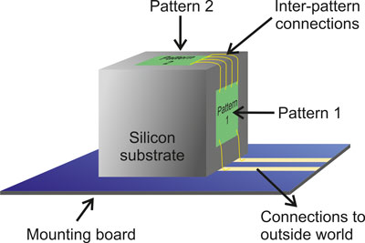 Fuente: |
Thursday, December 01, 2011
Breakthrough allows rapid, CMOS-compatible fabrication of large 3D photonic crystals
Subscribe to:
Post Comments (Atom)
NEODIMIO ¡no te lo pierdas!

-
 De entre todos los compuestos químicos que existen, quizá sean los llamados compuestos de coordinación los que mayores dificultades ofrecen ...
 -
Básicamente el video habla por sí sólo. Se tiene una cerveza fría líquida recién sacada del refrigerador o congelador, se le da un golpe y e...

No comments:
Post a Comment